Product Summary
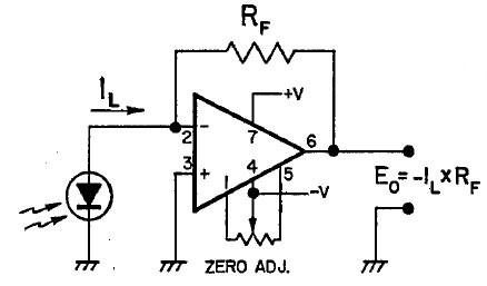
This series of p on n silicon diodes is primarily intented for use in the photovoltaic mode but may be used with a small reverse bias. The VTB5041B has excellent response in the uv region and units with uv transmitting windows are characteriaed 220nm. The VTB5041B has very high shunt resistance to provide very low offset in high gain transimpedance corinected op-amp circuits.
Parametrics
VTB5041B absolute maximum ratings: (1)Its storage temperature range would be from -40℃ to 110℃. (2)Its operating temperature range would be from -40℃ to 110℃. Those are all the main absolute maximum ratings. It should be noted that stresses above those listed in absolute maximum ratings may cause permanent damage to device.
Features
VTB5041B features: (1)enhanced uv to ir spectral range; (2)intergral ir rejection fliters available; (3)no uv enhancement; (4)response 220nm, 0.06a/w, typ with uv windows; (5)response 365nm, 0.14a/w typ; (6)high open circuit voltage low light levels; (7)1-2% linearity over 7 to 9 decades; (8)very low dark currents; (9)very high shunt resistance.
Diagrams

 |
 VTB5040B |
 Other |
 |
 Data Sheet |
 Negotiable |
|
||||
 |
 VTB5040J |
 Other |
 |
 Data Sheet |
 Negotiable |
|
||||
 |
 VTB5041 |
 Other |
 |
 Data Sheet |
 Negotiable |
|
||||
 |
 VTB5051 |
 Other |
 |
 Data Sheet |
 Negotiable |
|
||||
 |
 VTB5051B |
 Other |
 |
 Data Sheet |
 Negotiable |
|
||||
 |
 VTB5051BH |
 Other |
 |
 Data Sheet |
 Negotiable |
|
||||
 (China (Mainland))


