(China (Mainland))


Product Summary
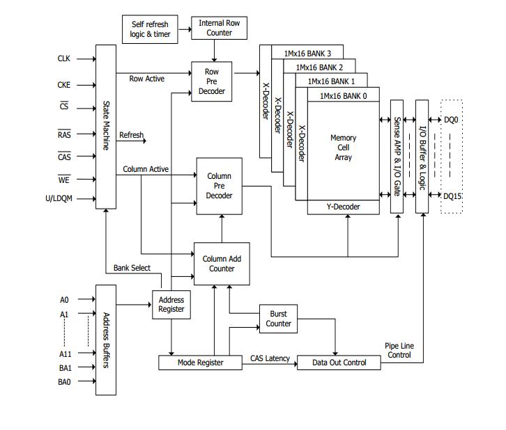
The Hynix HY57V641620ETP-6 is a 67,108,864bit CMOS Synchronous DRAM, ideally suited for the memory applications which require wide data I/O and high bandwidth. HY57V641620ETP-6 is organized as 4banks of 1,048,576x16. HY57V641620ETP-6 is offering fully synchronous operation referenced to a positive edge of the clock. All inputs and outputs are synchronized with the rising edge of the clock input. The data paths are internally pipelined to achieve very high bandwidth. All input and output voltage levels are compatible with LVTTL.
Parametrics
HY57V641620ETP-6 absolute maximum ratings: (1)Ambient Temperature: 0 ~ 70℃; (2)Storage Temperature: -55 ~ 125℃; (3)Voltage on Any Pin relative to VSS: -1.0 ~ 4.6 V; (4)Voltage on VDD relative to VSS: -1.0 ~ 4.6 V; (5)Short Circuit Output Current: 50 mA; (6)Power Dissipation: 1 W; (7)Soldering Temperature / Time: 260/10℃/sec.
Features
HY57V641620ETP-6 features: (1)Voltage: VDD, VDDQ 3.3V supply voltage; (2)All device pins are compatible with LVTTL interface; (3)54 Pin TSOPII (Lead or Lead Free Package); (4)All inputs and outputs referenced to positive edge of system clock; (5)Data mask function by UDQM, LDQM; (6)Internal four banks operation; (7)Auto refresh and self refresh; (8)4096 Refresh cycles / 64ms; (9)Programmable CAS Latency; 2, 3 Clocks; (10)Burst Read Single Write operation.
Diagrams